Design Procedure
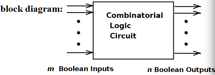
Combinational Circuits
基本结构:
- A set of m Boolean inputs
- A set of n Boolean outputs
- n switching functions, each mapping the 2m input combinations to an output such that the current output depends only on the current input values
设计思路:模块拆解(自顶上下) 设计预定义复用模块(IP核)
设计过程:
- Specification 调研:Write a specification for the circuit if one is not already available
- Formulation:Derive a truth table or initial Boolean equations that define the required relationships between the inputs and outputs, if not in the specification
- Optimization:Apply 2-level and multiple-level optimization
- Technology Mapping:Map the logic diagram or netlist to the implementation technology selected(门 -> 与非 / 或非)
- Verification:Verify the correctness of the final design manually or using simulation
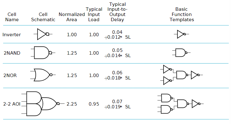
单元库:
- 原理图
- 占用面积
- 输入负载
- 传输延迟
- 映射模板
工艺映射:
- 假设:忽略门负载、门延迟;目标门与非门均可用
- NAND映射算法:
- AND:后加非 OR:前加非(\(A+B=\overline{\overline{AB}}=\overline{\overline A+\overline B}\))
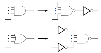
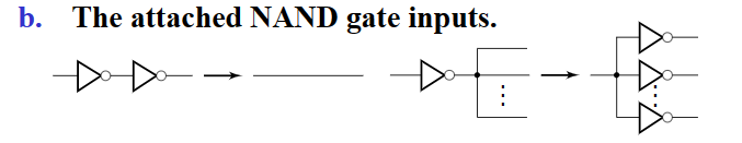
- 非门推过扇出点,两非门相互抵消
- 例:
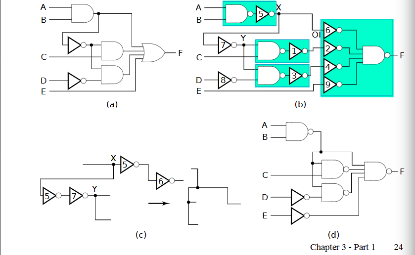
- AND:后加非 OR:前加非(\(A+B=\overline{\overline{AB}}=\overline{\overline A+\overline B}\))
- NOR映射算法:AND:前加非 OR:后加非
验证:
- 真值表
- 布尔方程
- HDL仿真
- 设计TestCase