Integrated Circuits
概念:Integrated circuit (informally, a “chip”) is a semiconductor crystal (most often silicon) containing the electronic components for the digital gates and storage elements which are interconnected on the chip.
分类:
- SSI (small-scale integrated) - fewer than 10 gates
- MSI (medium-scale integrated) - 10 to 100 gates
- LSI (large-scale integrated) - 100 to thousands of gates
- VLSI (very large-scale integrated) - thousands to 100s of millions of gates
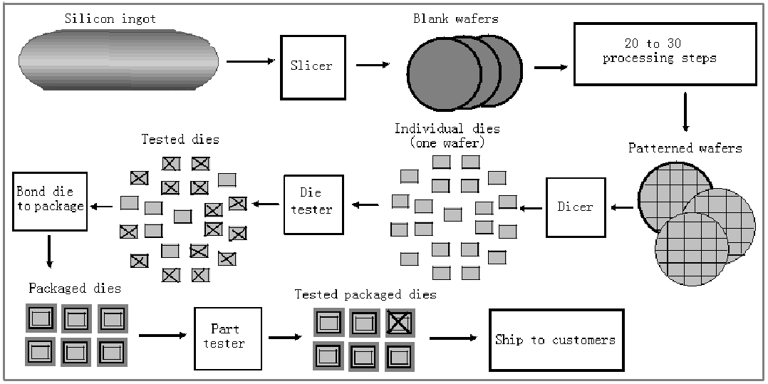
生产流程:
基本参数:
- 扇入系数:门驱动力大小,即一个门的输入数量
- 扇出系数:一个门的输出能带动多少门的输入
- 逻辑电平:
- 噪声容限:
- 传输延迟:输入改变到输出改变所需的时间
- 衡量:变化至H,L间50%的输入输出时刻的距离
- \(t_{PHL}\):输出\(H\to L\),\(t_{PLH}\):输出\(L\to H\)
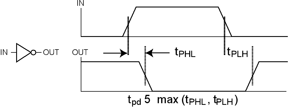
- \(t_{pd}:=\max\set{t_{PHL},t_{PLH}}\) or \(t_{pd}:=\dfrac{t_{PHL}+t_{PLH}}{2}\)
- 模型:
- 传输延迟:a change in the output in response to a change on the inputs occurs after a fixed specified delay
- 惯性延迟:rejects narrow “pulses” on the outputs (a time interval less than the rejection time)
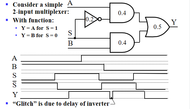
- 竞争冒险:由于传输延迟造成的形如\(^{^{^{\_\_}}}\!\vert\!_{\_\_}\!\vert\!^{^{^{\_\_}}}\)的跳变(由于惯性延迟的存在,实际不会出现)
- 扇出负载对传输延迟具有影响:如\(t_{pd}=0.07+0.021SL\)
Other Gate Types
Buffer门:
- 定义:\(F=X\)
- 作用:信号放大器,提高扇出能力与操作速度
NAND门:
- 定义:\(F(X,Y,Z)=\overline{XYZ}\)
- 性质:\(\overline{XYZ}=\overline{X}+\overline{Y}+\overline{Z}\),AND-Invert and Invert-OR both represent the NAND gate
- 作用:通用逻辑门,可实现任意电路
NAND无结合律,运算复杂,一般先设计普通门电路再映射至NAND用于生产
NOR门:
- 定义:\(F(X,Y,Z)=\overline{X+Y+Z}\)
NOR门即为NAND门对偶门
异或 / 同或门:
- 定义:\(X\oplus Y=X\overline{Y}+\overline{X}Y,\overline{X\oplus Y}=XY+\overline{X}\overline{Y}\)
| X | Y | X\(\oplus\)Y |
|---|---|---|
| 0 | 0 | 0 |
| 0 | 1 | 1 |
| 1 | 0 | 1 |
| 1 | 1 | 0 |
| X | Y | Z = \(\overline{X\oplus Y}\) |
|---|---|---|
| 0 | 0 | 1 |
| 0 | 1 | 0 |
| 1 | 0 | 0 |
| 1 | 1 | 1 |
- 性质:\(X\oplus Y\oplus Z=\overline{X}\overline{Y}Z+\overline{X}Y\overline{Z}+X\overline{Y}\overline{Z}+XYZ\)
- 恒等式:
- \(X\oplus0=X\qquad X\oplus1=\overline{X}\):利用该原理控制是否为非门
- \(X\oplus X=0\qquad X\oplus\overline{X}=1\)
- \(X\oplus Y=Y\oplus X\qquad (X\oplus Y)\oplus Z=X\oplus(Y\oplus Z)=X\oplus Y\oplus Z\)
- \(X\oplus\overline{Y}=\overline{X\oplus Y}\)
奇偶函数:
- 定义:The 1s of an odd function correspond to minterms having an index with an odd number of 1s.(卡诺图交错排布)
- 实现:异或门 \(F=X\oplus Y\oplus Z=(X\oplus Y)\oplus Z\)
- 应用:生成纠错码(纠错码与原码1总和个数奇偶性确定,故带入奇函数输出确定)
高阻态:
- 三态门:0, 1, 高阻(Hi-Z)
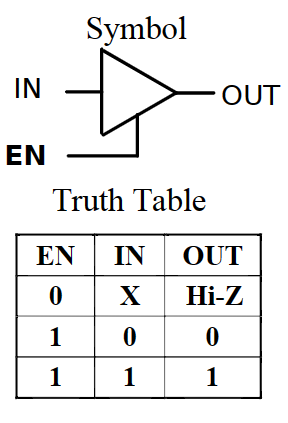
- 原理:未接入电路(接高低电平的CMOS均断开)
- 作用:可串联输出(总线上有且仅有一个门能正常工作,其余处于高阻态以保护电路)
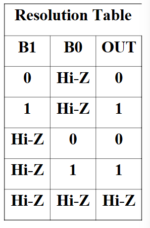
- 应用:多路选择器 控制使能控制选择
AOI电路:
- 记法:输入个数-门个数-...-
- 例:2-2-1AO 两输入2与门1或门电路